

RCR Wireless
  • News
  • Channels
    • 5G
    • 6G
    • BSS OSS
    • Carriers
    • IoT
    • Network Infrastructure
    • Open RAN
    • Private 5G
    • Telco AI
    • Telco Cloud
    • Test & Measurement
  • Resources
    • Reports
    • Webinars
    • White papers
    • AI Fundamentals
    • Analyst Angle
    • Editorial Calendar
    • Fundamentals
      • 5G NR Release 17
      • AI
        • Telco AI in 2025
    • Podcasts
      • Let’s Get Digital with Carrie Charles
      • Wireless Connectivity to Enable Industry 4.0 for the Middleprise
      • Well Technically…
      • Will 5G Change the World
      • Accelerating Industry 4.0 Digitalization
  • AI Infrastructure
  • Programs
  • Events
  • RCRtv
  • Advertise
  • Subscribe
Monday, August 31, 2026
RCR Wireless
  • News
  • Channels
    • 5G
    • 6G
    • BSS OSS
    • Carriers
    • IoT
    • Network Infrastructure
    • Open RAN
    • Private 5G
    • Telco AI
    • Telco Cloud
    • Test & Measurement
  • Resources
    • Reports
    • Webinars
    • White papers
    • AI Fundamentals
    • Analyst Angle
    • Editorial Calendar
    • Fundamentals
      • 5G NR Release 17
      • AI
        • Telco AI in 2025
    • Podcasts
      • Let’s Get Digital with Carrie Charles
      • Wireless Connectivity to Enable Industry 4.0 for the Middleprise
      • Well Technically…
      • Will 5G Change the World
      • Accelerating Industry 4.0 Digitalization
  • AI Infrastructure
  • Programs
  • Events
  • RCRtv
  • Advertise
  • Subscribe
Add RCR Wireless as a preferred source on Google
  • Qualcomm 6G Insights
  • Huawei Content Hub
  • Qualcomm – 6G Vision
  • OSS/BSS Channel
  • RCRTech Roundtable: AI Infrastructure
RCR Wireless
RCR Wireless
  • Advanced Mimo
  • Mobile mmWave
  • 5G Positioning
  • Green Networks
  • Metaverse
  • Automotive
  • Industrial and Wide-area IoT
Copyright 2021 - All Right Reserved
Home - Making mobile chips – a sneak peek at wafer manufacturing
Chips - SemiconductorWireless

Making mobile chips – a sneak peek at wafer manufacturing

by sylvie barak July 26, 2010
written by sylvie barak July 26, 2010 Share
LinkedinEmail
Share 0LinkedinEmail
149

.
Most people don’t give too much thought to the tiny components which form such an integral part of almost all modern communication devices, from PCs to mobile phones.
Indeed, mobile chips get almost no public recognition in a world which seems to care more about screen size, shiny aluminum casings and apps – yet without powerful application processors, our handsets and devices would be nothing more than bricks.
Making chips, however, is no easy task, nor is it a cheap one, resulting in many firms choosing to outsource their manufacturing to dedicated “fabs” to feed the almost insatiable modern appetite for smaller, faster processors.
In Singapore recently, RCR was privileged to be able to get a glimpse behind the chipmaking curtain at GlobalFoundries’ fab 7, where wafer upon wafer of chips are churned out daily from within the impressive maze of cleanrooms.
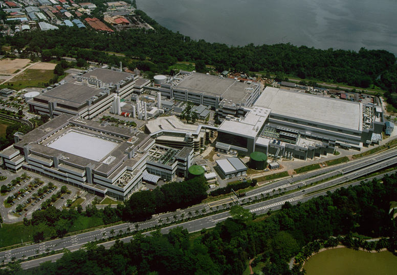
fab7

GlobalFoundries’ expertise is in producing very small, very power efficient chips based on the ARM architecture and   Fab 7 manufactures mobile products for many of the world’s largest wireless chip companies including Qualcomm, Broadcom, Atheros and many others.
Getting a grand tour of the facility, VP of Fab 7 Peter Benyon explained the magic behind the process as well as the inherent paradoxes of balancing the need for increased performance with lower power and heat, larger die sizes at lower costs and how increased complexity can have a negative impact on wafer yields.
The process of making a wafer can take two to three months and involves a number of steps including film deposition (Oxidation, DCVD & PVD), chemical mechanical polishing (CMP), photolithography, etching, cleaning technology, implantation and diffusion.  Each of these is a process in and of itself, and can be repeated several times in fixed order.
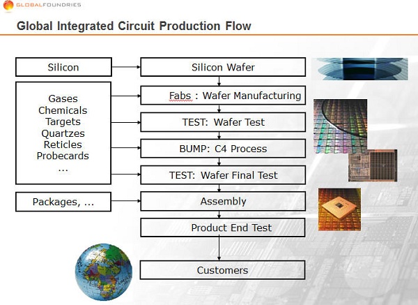
makingchips1

After the initial polishing phase, photolithography is where the actual chipmaking really begins, as the pattern is projected onto the wafer like an optical mask. That creates a pattern in the etching resist which is then exposed to light, to dissolve parts of the substrate in a process similar to the one that occurs in photography.
lithography1

The next stage is Plasma Etching, in which a high-speed stream of glow discharge (plasma) gas is shot at the wafer in bursts. After a while, the atoms embed themselves at or just below the surface of the target and modify its physical properties.
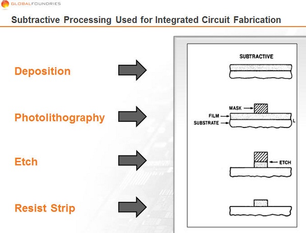
etch1

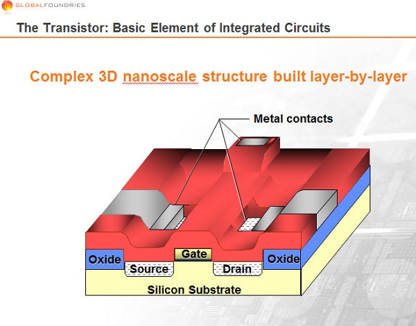
After etching comes yet more cleaning before the wafer arrives at the implant phase where a controlled amount of impurities is added to the silicon structure in order to improve electrical conduction, in a process similar to shooting bullets into walls. Diffusion then drives the impurities further into the silicon structure so that the good electrical conducting area becomes bigger.
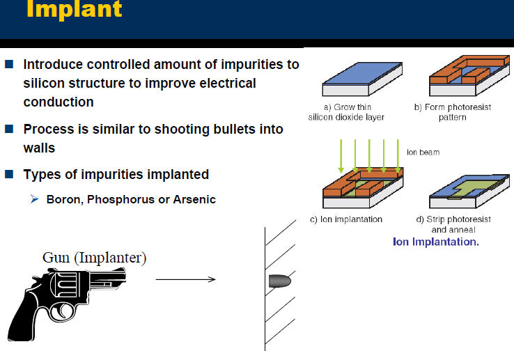
implant

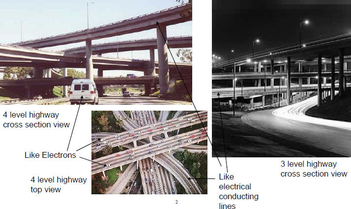
Typically, each wafer goes through 33-50 mask levels and 500- 800 processing steps and by the end, with its multiple layers and levels, wafer fabrication can be likened to building multi-level highways.
highway

transistor
So next time you pick up your phone, you might want to marvel at the sheer amount of work and complexity that went into making its smallest, but most important, component – the processor chip.
Check out RCR’s slideshow from inside Fab 7 below:


You Might Also Like
  • Softbank targets sovereign AI demand in Japan
  • Verizon’s Srini Kalapala on betting on AI and edge computing
  • T-Mobile bets on hybrid broadband with 5G FWA and Starlink
  • SpaceX brings Xsight Labs onboard ahead of Starlink v3 launch
  • Emerson/NI White Paper: 2026 Technology Trends Impacting the Wireless Communications Industry
  • The hidden pattern in Nvidia’s billion-dollar deals (Analyst Angle)
Share 0 LinkedinEmail
sylvie barak

previous post
Jailbreaking cool according to Library of Congress
next post
Eight million Windows Phone 7's for AT&T

White Papers

  • Norton eBook: The 2026 Telco Playbook

  • Enea White Paper: Why Intelligent AAA is the Swiss Army Knife of Telecom

  • CSG White Paper: Telco AI Enabler: Mediation’s Defining Role

  • Enea White Paper: Scalable Database Design for 5G and Beyond

  • Supermicro and NVIDIA Whitepaper: Powering sovereign AI at scale

Editorial Reports

  • Report: Rethinking the RAN

  • Report: Building AI-Era Network Fabrics

  • Quantum Safe Networks Market Pulse Report

Webinars

  • Mimosa Webinar – Build the Right Network

  • Webinar: Building 6G — aligning technology, policy and purpose

  • SIMCom Webinar: Scaling your next deployment – from plastic to provisioning

  • Webinar: Rethinking the RAN as AI, cloud and openness converge

  • Webinar: Scale-Up, Scale-Out, Scale-Across – Building AI-Era Network Fabrics

Since 1982, RCR Wireless News has been providing wireless and mobile industry news, insights, and analysis to mobile and wireless industry professionals, decision makers, policy makers, analysts and investors.

Facebook Twitter Youtube Linkedin Envelope Rss

Useful Links

  • Subscribe
  • About RCR Wireless News
  • Contact Us
  • Advertise
  • Editorial Calendar
  • Archive
  • RSS
  • Wireless News Archive
  • Subscribe
  • About RCR Wireless News
  • Contact Us
  • Advertise
  • Editorial Calendar
  • Archive
  • RSS
  • Wireless News Archive

Edtior's Picks

AT&T takes OTel 2.0 into production
Report: Rethinking the RAN
How space traffic management can save our satellites (Reader Forum)

Latest Articles

AT&T takes OTel 2.0 into production
Report: Rethinking the RAN
How space traffic management can save our satellites (Reader Forum)
Verizon and Google Cloud expand AI partnership across service, network, and data

© 2026 RCR Wireless News All Right Reserved. Developed by Eight Hats.

Cookie Policy | Privacy Policy

RCR Wireless
  • News
  • Channels
    • 5G
    • 6G
    • BSS OSS
    • Carriers
    • IoT
    • Network Infrastructure
    • Open RAN
    • Private 5G
    • Telco AI
    • Telco Cloud
    • Test & Measurement
  • Resources
    • Reports
    • Webinars
    • White papers
    • AI Fundamentals
    • Analyst Angle
    • Editorial Calendar
    • Fundamentals
      • 5G NR Release 17
      • AI
        • Telco AI in 2025
    • Podcasts
      • Let’s Get Digital with Carrie Charles
      • Wireless Connectivity to Enable Industry 4.0 for the Middleprise
      • Well Technically…
      • Will 5G Change the World
      • Accelerating Industry 4.0 Digitalization
  • AI Infrastructure
  • Programs
  • Events
  • RCRtv
  • Advertise
  • Subscribe
RCR Wireless
  • News
  • Channels
    • 5G
    • 6G
    • BSS OSS
    • Carriers
    • IoT
    • Network Infrastructure
    • Open RAN
    • Private 5G
    • Telco AI
    • Telco Cloud
    • Test & Measurement
  • Resources
    • Reports
    • Webinars
    • White papers
    • AI Fundamentals
    • Analyst Angle
    • Editorial Calendar
    • Fundamentals
      • 5G NR Release 17
      • AI
        • Telco AI in 2025
    • Podcasts
      • Let’s Get Digital with Carrie Charles
      • Wireless Connectivity to Enable Industry 4.0 for the Middleprise
      • Well Technically…
      • Will 5G Change the World
      • Accelerating Industry 4.0 Digitalization
  • AI Infrastructure
  • Programs
  • Events
  • RCRtv
  • Advertise
  • Subscribe
@2020 - All Right Reserved. Designed and Developed by PenciDesign