“5G” networks are expected to unleash solutions that will help overcome barriers to widespread internet of things adoption. Existing technology limitations lead to high connectivity costs, and security and privacy concerns. A shared vision of the pillars of 5G networks includes ubiquitous high-speed internet access, massive IoT and machine-to-machine communications for critical missions. To achieve that we need to increase bandwidth, reduce latency and release scalability, as well as reduce deployment-and-operation costs.
Leveraging millimeter waves above the 24 GHz band will open up an extra spectrum resource for infrastructure and possibly radio access network. This extra spectrum is a breath of fresh air. However, end-to-end capacity of mobile networks cannot be increased indefinitely with extra resources. Providing the expected quality of experience of 5G networks requires a cross-layer “softwarization” that can provide the right resources at the right place and at the right time. The leap to 5G is so big it will require disruptive microelectronics and nanotechnologies for both radio frequency and digital platforms.
Softwarization with SOI-based technology
5G will require ultra-dense networks to ensure sufficient quality of service for the exponential increase of users and machines. New critical missions will require computing resources to be located as close as possible to applications to ensure zero-latency responses. The primary idea of 5G mobile network architecture is cloud-RAN with physically centralized baseband processing and distributed multiple radio heads. The critical fronthaul connectivity interface calls for advanced digital baseband, i.e. massive multiple-input/multiple-output schemes and carrier aggregation. This deployment requires new digital platforms as the deployment of small cells in wide area networks must be addressed in a business-sustainable way. Base station architecture should be modified for high flexibility with a generic hardware footprint.
CMOS technologies are key enablers of 5G infrastructure, which calls for pervasive digital resources. Silicon-on-insulator technology shows promising capabilities for flexibility and scalability in digital deployment. Beyond bulk CMOS, fully depleted SOI transistor technology has better electrostatic performance, which enables ultra-low voltage optimization. FDSOI technology also opens a new landscape for designers thanks to its efficient modulation of threshold voltage. One device can reach a large range of applications from high-performance burst modes to very low power. Innovative design-and-control algorithms allow benefits from SOI as a softwarization of hardware footprints can meet diverging needs in the IoT. Furthermore, RF SOI technology reduces the cost of integration of multiple radio access technology options in one programmable device.
Reaching the mm waves
The mm wave air interface remains a challenge. High-gain smart antennas are required to deploy mm wave communication in practical fields. MIMO beamforming techniques are needed to ensure a sufficient QoS in mobile and multipath propagation scenarios. The power consumption of 5G systems will be a major issue due to the very large number of antennas and ultrawideband digital baseband. Consequently, hybrid beamforming architectures should be defined with respect to different possible options of digital/analog partitioning and software implementation. The promising performances of FDSOI devices at 24 GHz lead the research towards digital and mm wave RF co-integration. As the final performances depend on close integration of antennas and RF devices, 3D packaging is a key enabling technology to optimize partial integration of mm wave smart antennas.
Subscribe now to get the daily newsletter from RCR Wireless News
High power is critical for long-range mm wave backhauling as well as linearity for high throughput. “III-V” semiconductors are already used for high-end applications such as radar and military communications, etc. Gallium nitride promises robust, sustainable and low-cost materials for 5G mm wave high-power applications. Current research projects are investigating possible GaN-on-Si technology to enable low-cost integration of high-power mm wave devices.
Technology for 5G verticals
There is a new complexity in the technology roadmap since the transistor takes part of advanced system architectures where the software component is increasing. We do not continue focusing on tinier transistors only when technology roadmaps call for heterogeneous integration, advanced packaging and new materials. After two decades of smartphones driving integration of more computing with lower power, diverging IoT services that require innovative flexibility and scalability from the technology add new challenges for 5G systems.
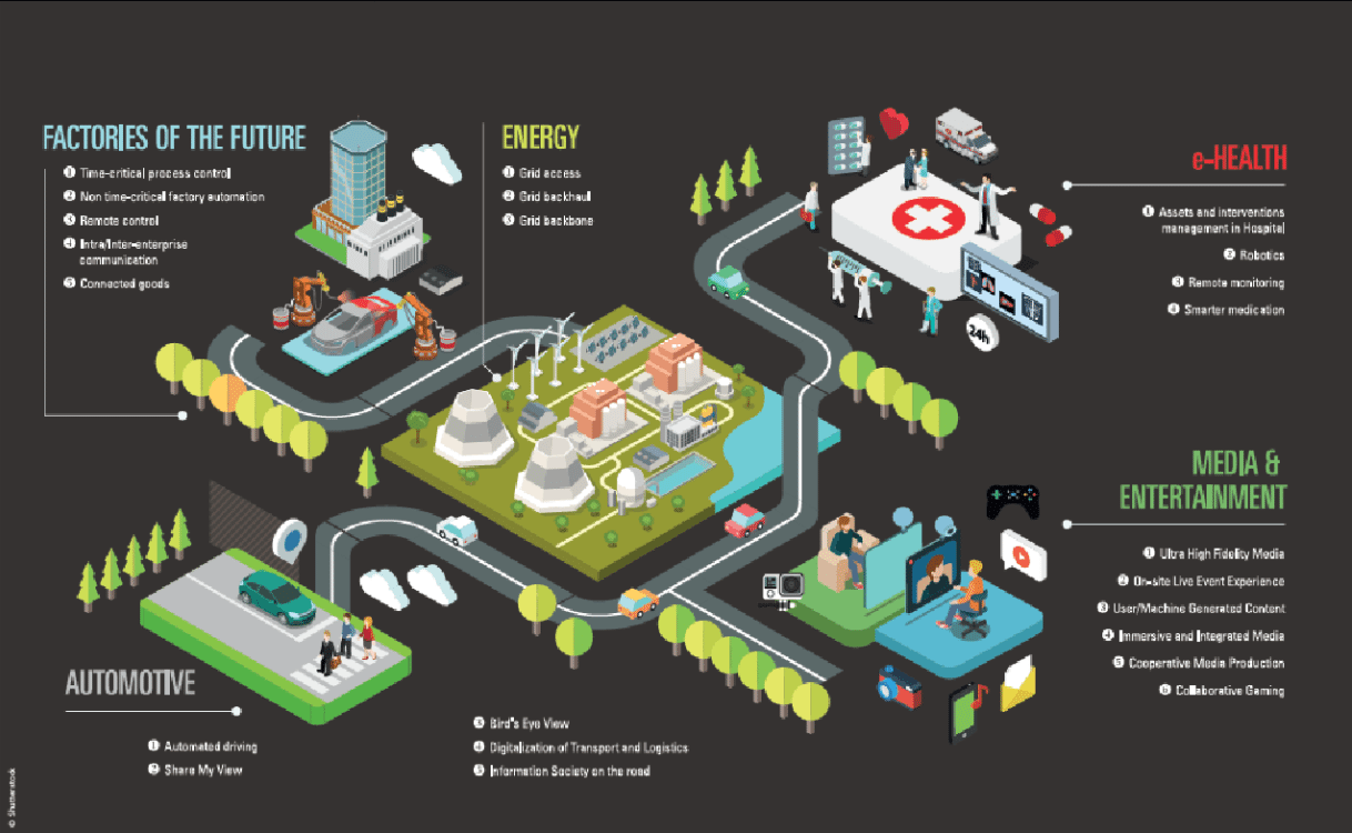
The complexity of future 5G networks will require self-organized networks and smart applications. Consequently, most 5G nodes should be part of the distributed network management by collecting and analyzing contextual cyber-physical information. There is a new paradigm that calls for a close cooperation between infrastructure and applications. The leading requirements on 5G integrated systems will come from 5G verticals such as automotive, smart cities, utilities, smart industry, etc.
These industries must share their roadmaps and participate in research and development frameworks with 5G technology experts if they want to reap the benefits of future networks.

Editor’s Note: In an attempt to broaden our interaction with our readers we have created this Reader Forum for those with something meaningful to say to the wireless industry. We want to keep this as open as possible, but we maintain some editorial control to keep it free of commercials or attacks.

