Fabless semiconductor startups are making interesting 5G silicon by converting big ideas into practice
5G is a complex problem: how to create 100x faster networks that can handle 1000x more traffic with low latency using fewer, and sometimes more problematic, resources. Spectrum is a finite resource to be shared or divvied up (or both). Add to that the nature of certain bands that require extra effort to work over distance or in the face of physical environment obstacles.
Startups have been developing and making integrated circuits that may tackle aspects of the 5G problem for years. From the network architecture to the user’s device, every aspect of 5G has a problem to solve.
[Read RCR Wireless News‘ Roadmap to 5G.]
Occasionally, RCR Wireless News will feature chips used in 5G, to show the variety of silicon that’s now (or soon to be) 5G ready. Here are three companies to watch.
Beamforming: Anokiwave Inc.’s active antenna ICs for wideband beamforming
The problem:
We know millimeter wave spectrum will be used in 5G. Tiny waves at high frequencies — it’s just the nature of mmWave to be both fast and easily inhibited by any kind of physical obstacle, even a rain shower. Beamforming, the focusing of the downlink waves to a target, will be a key in making this waveform work.
The chip(s):
“Beamforming is not new technology and has been around a long time, but now we are industrializing it for 5G use,” said David Corman, chief system architect at Anokiwave, in a report. “These are not lab curiosity parts. They are ready for prime time.”
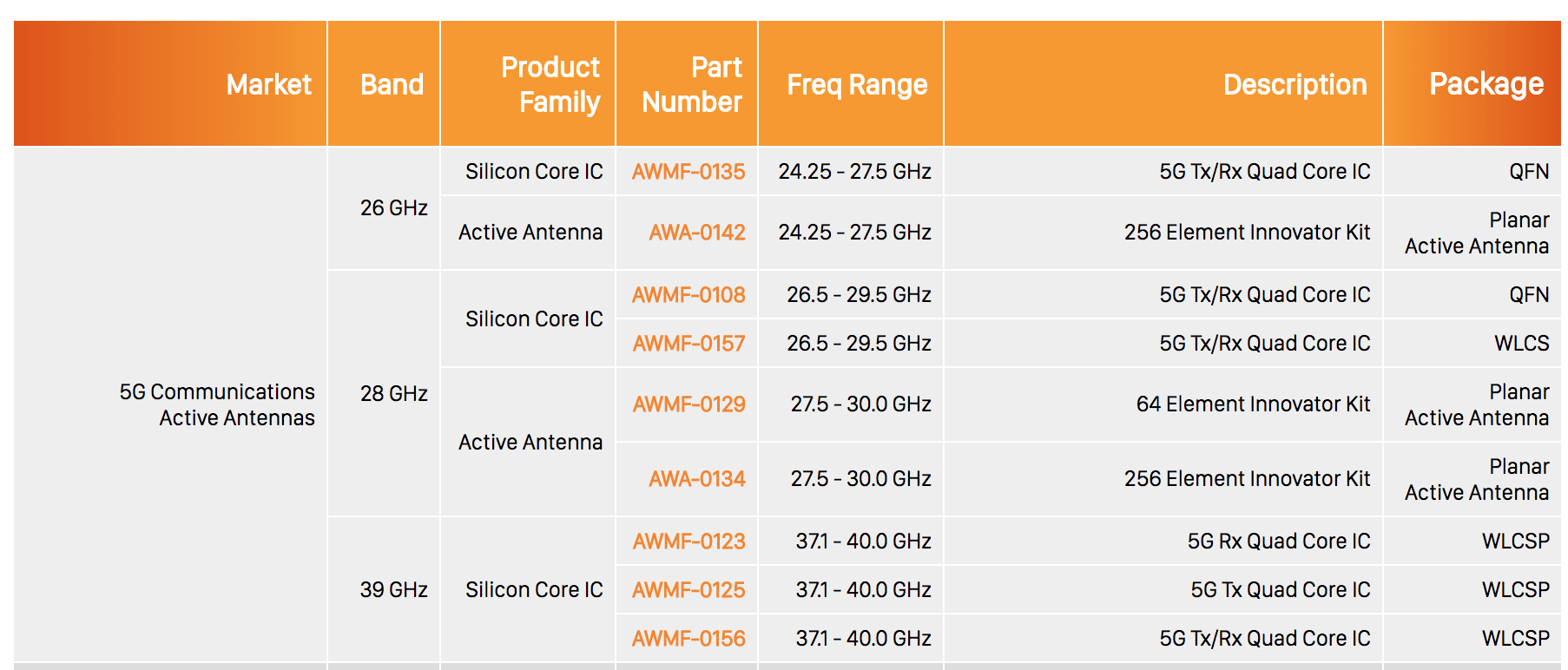
5G Silicon Quad Core ICs include the 28 GHz AWMF-0157 IC and the 39 GHz AWMF-0156 IC, both announced in February 2018. The chips control phased-array antennas and are ready to go into Third Generation Partnership Project-compliant base stations. They both support four radiating elements, have gain and phase controls for analog radio frequnecy beam steering, and Anokiwave’s special sauce IP blocks for low-cost hybrid beamforming.
- 28 GHz AWMF-0157 IC operates at 26.5 – 29.5 GHz
- 39 GHz AWMF-0156 IC operates at 7.1 – 40.0 GHz
Other chips for 5G are mmW Phased Array Antenna Innovator’s Kits with Anokiwave’s AWMF-0135 26GHz 5G Quad Core IC (announced in November 2017).

How they are used now:
Used in the aerospace and defense industries for decades, Anokiwave’s silicon for phased-array antennas has been tweaked for 5G and is in companion arrays, such as Anokiwave’s reconfigurable 256-element Active Antenna, the AWA-0134. AWA-0134 is a 256-element phased-array at 28 GHz for use in real-time active beam-steering applications in a single 256-element or in a 4×64 element configuration that enables 4×4 MIMO testing. A blog on Anokiwave’s website says that “the AWA-0134 was the first commercially available 256-element phased-array at 28 GHz.”
[What is millimeter wave? Read an explanation on RCR Wireless News.]
The company saw the 5G light years ago and started adapting its mil/aero business into commercial 5G potential. “Learnings from the A&D and SATCOM markets have been applied to the fast and furious 5G market,” writes David Corman, the company’s chief systems architect, in a blog. “Our team has seen the importance of working directly with end users to fully understand what their pain points are and what they really want in an IC, so we can evolve architectures accordingly. This allows us to build a product that’s effective immediately for mmWave 5G applications.”
The company:
The company started in 1999 by founding member Deepti Jain. Headquartered in San Diego, CA, with design centers in Phoenix, AZ and Boston, MA. Crunchbase says it is a late-stage venture with Series C funding.
High densification: Edgewater Wireless’s WiFi3: multichanneling WiFi in high-density
The problem:
Sending Wi-Fi signals over single channels with one radio — how it works now —will not cut it in the 5G future, when we’re overcrowded with devices and interference, says Edgewater Wireless — and the company adds that beamforming is not the answer.
“In Wi-Fi, beamforming works great with a very few number of users, such as five users on an access point,” Andrew Skafel, president and CEO of Edgewater Wireless told RCR Wireless News. “It is typically downlink only. There’s limited application for it. There are definitely some places where it works very well, like in a nice confined basement where you have very little interference, and very few devices.”
The issue with beamforming and multiple-input multiple-output in a high-density environment is that together they splay the signal omni-directionally, said Skafel.
Regarding the basement: “The interesting thing is that is really where the [WiFi] standard was initially developed for,” said Skahel. “WiFi was meant to be the poor cousin you used in your basement. You wanted to get from your laptop to your DSL modem, or whatever, and that’s the premise in which it was developed. We’ve tried to make it faster and faster and faster assuming that environment hasn’t changed, and it really has.”
The chip:
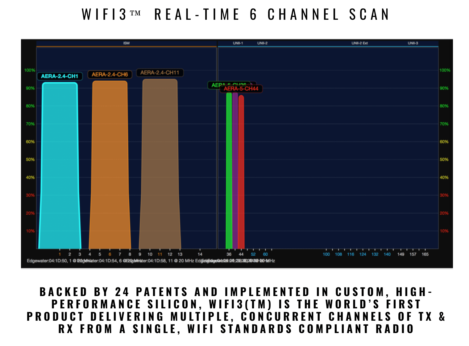
Wi-Fi3 chipsets have multiple, concurrent channels of transmit and receive from a single WiFi-standards-compliant radio. Edgewater uses its PowerZoning, which enables primary and secondary channels to avoid the channels overlapping when deploying access points in near each other.

WiFi3 does not rely on MIMO. “MIMO is using multiple antennas. In high-density environments, MIMO and beamforming act like omni-directional antennas and splay interference all around the access point,” said Skafel. “Whereas our approach has been very similar to a cellular network: Use directionality and focus the energy where you need the coverage, which has the dual effect of giving you better performance and it also reduces interference on all those other access points around.”
Skafel cites an IEEE paper that says you can get up to 500x better performance running multiple 20 MHz channels vs a couple of 160 MHz channels in a given area in high density. “What we will see is 5G will follow exactly the same fashion. You are much, much better off giving a narrow channel to as few devices as possible,” he said.
Edgewater manufactures the chip in the U.S. at Globalfoundries in New York State.
How is it used now:
The WiFi3 chips are in an access point, called Aero, and a mesh network, called MESHD. Both are available commercially. The company also licenses its technology and, of course, sells the chips. WiFi3 is also deployed in Kroger stores.
The company:
Ottawa, Canada–based Edgewater Wireless started in 1988. It is a publicly traded company. UpRamp, CableLab’s accelerator, recently selected Edgewater as a promising technology company for its Fiterator program, which the company has since competed.
Network programmability: Barefoot Network’s Tofino programmable network switching chip
The problem:
Mobile network operators will need data centers to scale their networks but scaling a network is not trivial. High-speed, high-performance networks are built on infrastructure that in the past had to be ripped out when moving up a node from 3G to 4G. Network hardware relies on ASICs — application-specific integrated circuits that are designed for one specific purpose and are fixed function — to power the hardware on the network. The fixed functions mean the networks can run fast but any changes to the network are labor intensive and take a long time. Some network hardware is programmable but only at the top of the of line, in hardware that costs millions of dollars, with hundreds of chips.
Part of the problem is networking is playing catch up. “Networking is not a fast-moving industry,” said Ed Doe, VP, product, business and strategy at Barefoot Networks, in an interview with RCR Wireless News. Whereas computing and storage has made leaps in innovation and processes, networking has been slow to change.
The chip:
Programmable switch chips will save time and money, says Doe. Barefoot’s Ethernet switch chip Tofino is programmable with the open-source P4 language — a language and API still developing now as Linux projects. The data plane, where all the traffic runs, separates from the control and management planes. Also built in, or added on, is in-band network telemetry (INT), where each packet collects and reveals telemetry about its journey. The visibility into the network will take the guess work out of troubleshooting the network.

Barefoot makes the case that Tofino (an ASIC) could be used throughout the network, including the edge. “The big trend is that more and more technology that has worked for large-scale data centers … are now starting to get brought into other markets,” said Doe. “One is into the 5G core infrastructure side of things … 5G extends that edge of the network. You are talking about distributing these workloads throughout the network and to the edge, instead of having them all sit in a central office.” Tofino is a chip used in data centers, that Barefoot Networks says is perfect for 5G networks.
More about Tofino:
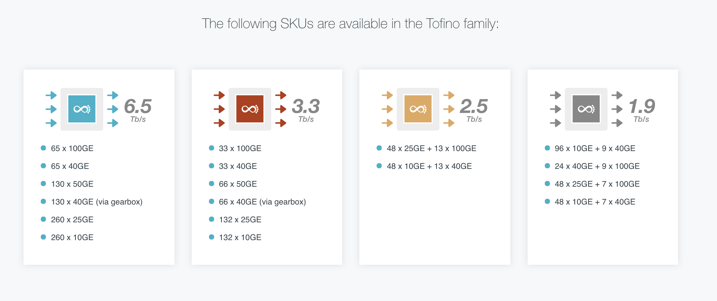
- Barefoot says Tofino is the fastest programmable switch chip in now production with processing at 6.5 terabits per second. (Some other chips are clocking faster but aren’t in production and aren’t programmable.)
- Runs Google’s tor.p4 forwarding plane program and P4 Runtime Agent
- ONOS acts as control plane for Tofino with P4 Runtime support
- SRv6 forwarding plane functionality. Interoperability demonstrated with Cisco products, open source implementations of SRv6
- Manufactured it at TSMC on 16nm process. (Most of the networking switch chips are made in 16nm process, which isn’t a cutting-edge node — but that is okay, say Doe. “It seems the cell phone guys tend to drive the newer, smaller processes first because they are concerned about [being on the forefront of reducing] power consumption,” he said.)
How is it used now:
High-speed, high-bandwidth users such as data centers and hyperscalers (Google for example) use the chip currently.
The company:
Barefoot Networks, founded in 2013, emerged from stealth mode in 2016. It has backing from Google, Microsoft, Intel, among others. Projects with P4 programming language came first, with the goal of creating a chip that could handle the programming. With P4, operators can make changes in software in a matter of hours. “The only way to make this happen was to make it an open source language that everyone could get behind,” said Doe. Over 100 companies support P4 efforts.
More info: Barefoot Networks’ Tofino was profiled last year by RCR Wireless News.

