SANTA CLARA, Calif. — 3D chips are the next frontier for machine-learning chip design, said Globalfoundaries CTO of ASICs, at the IoT DevCon and Machine Learning Conference this week.
Wireless networks and equipment on them, even internet of things equipment, will likely have machine learning and artificial intelligence in the near future. Special chips are being designed now that can handle the computational load of machine learning. But be warned: these chips are big.
Machine learning requires a large dataset from which to train the machine — a machine can’t learn without being trained. Image identification is a good example. Humans create the data set by tagging thousands of pictures — for instance, identifying which photos are of cats versus dogs. The pictures can then be used to train algorithms so the machine can take over identifying cats versus dogs. The data sets are key to making machine learning work.
The machine learning-enabled chips are going to be complex, which will cause issues with design.
“The problem is, if you were a software team who was happy working with FPGAs and GPUs, now you need a full design team,“ said Igor Arosvksi, CTO of ASIC business at the semiconductor manufacturer Globalfoundries. ”A lot of companies are struggling with that barrier.”
The ASIC (application-specific integrated circuit) is a purpose-built chip, designed for the device or devices it will be used in. It is not a generic type of chip, such as an FPGA or microcontroller, which may have flavors to go with certain devices but aren’t specifically designed and optimized for one specific device. ASICs usually cost more because they require custom development, and a lot can go wrong along the way. They also work well and may be the only option in some cases. Machine learning chips are now frequently made as ASICs.
Arosvksi described some of the processes available and that Globalfoundries can help with the complexity of ASIC design, which is a stumbling block; the company can support up to 25 designs, he said. Customers’ intellectual property (IP) is needed for the competitive system in this market, said Arosvksi.
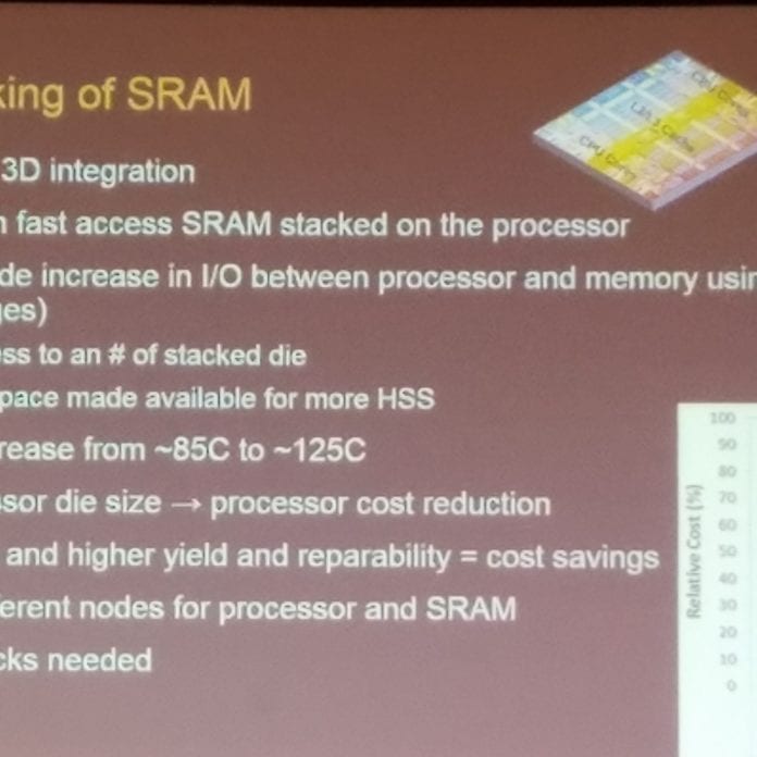
The 3D chips use separate stacked dies that each serve a different purpose. 3D SRAM stacks on logic will enable an order of magnitude leap in interconnect density and power, said Arosvkski. Also one can be choosy when chips are stacked: the stack layers can be tested separately, with only the best chips married to the stack. Because the separate sections are not on one chip, you don’t have throw away the stack if one layer is bad.
The memory in the stack, often as SRAM, which can take more heat. Interestingly, “the access to memory is really the most energy-consuming task,” said Arosvkski. “It really is not just the compute, but is it really moving that data in and out of memory. This is where you consume a lot of the energy. This is both a big challenge and an opportunity.”
A chip’s packaging will also be important to AI’s future: Although Moore’s Law is slowing down, it continues in packaging, and Arosvkski said that some innovations that may improve chip performance leverage packaging.

