NXP exec: ‘With GaN technology, 5G systems can be built with extended power and bandwidth’
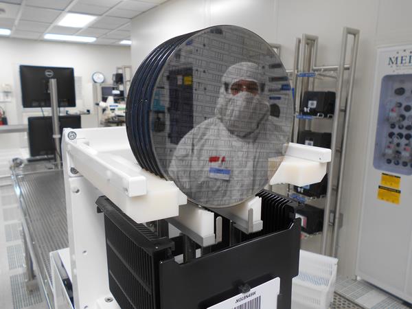
Following NXP Semiconductor’s news that it has opened a 150 mm (6-inch) RF Gallium Nitride (GaN) fab in Chandler, AZ, RCR Wireless News spoke with the company’s Executive Vice President and General Manager of Radio Power Paul Hart to find out more about the decision to open the new factory, as well as what makes RF GaN technology suited for 5G RF power amplifiers.
“What we really wanted to do,” Hart began, “was more tightly couple this GaN technology, which we saw as being a key tech element for 5G applications, with the product development teams and the system teams inside NXP, so—like what we’ve done over the last 20 years with silicon—we could rapidly innovate and develop the technology.”
“Therefore, we made the decision to invest in this factory here in Chandler,” he added.
NXP’s development of Gallium Nitride, which is a compound semiconductor technology that the company says is better suited for high-power applications, started in 2000. The technology goes into cell tower base stations and according to Hart, its goal is to “make the little RF signals really big.”
“As we migrate from 4G to 5G, the whole industry has to move to wider bandwidth spectrum and up in frequency where more spectrum is available in order to increase the data rates and lower latency,” explained Hart. “What was obvious was that the workhorse of the past, LDMOS, starts to run out of steam in terms of performance as you get above many of the conventional frequency bands.”
Because GaN is a large-band gap technology, it is possible to have a large electric field generated within the technology. Further, GaN also allows for a high-frequency response and a high-power density simultaneously.
“It enables more power at higher frequency than we could in the past with the same amount of power consumption,” summarized Hart.
He went on to say that GaN’s advantages really shine when it comes to mid-band — 2.6 and 3.5 GHz — spectrum. This is specifically where the efficiencies of LDMOS begin to wane, and where there is much better efficiency from GaN.
“What that means is these more complicated 5G systems can be built with extended power and bandwidth to deliver these high-data-rate, low-latency signals,” Hart said.
The factory is expected to reach full capacity by the end of 2020 and will serve as an innovation hub, facilitating collaboration between the fab and NXP’s onsite R&D team.
Last year, NXP furthered its commitment to communication infrastructure with the purchase of Marvell’s Wi-Fi, Bluetooth and other wireless connectivity business assets for $1.76 billion. NXP said at the time thatthe acquisition will allow the company to offer its customers wireless connectivity solutions that include Wi-Fi 4, 5 and 6 and Bluetooth/BLE along with NXP’s flagship edge computing platforms for “comprehensive, turn-key solutions for the Industrial & IoT, Automotive and Communication Infrastructure markets that simplifies customers’ supply chain logistics and improves time-to-market.”

