With today’s global migration to 5G, mobile wireless communication is undergoing a renaissance. The roll-out of innovative new mmWave technology as part of that technology stack is helping to drive the adoption of 5G, as mmWave promises to increase data rates and provide a superior network experience to current and future cellular subscribers. This is because mmWave can offer an improvement in data rates in excess of 10x compared to traditional sub-6 GHz links. That translates to faster downloads (and uploads) that can alleviate the worst effects of network congestion. When connected to an mmWave band, for example, subscribers will immediately notice that video loads faster, even in high-resolution 4K formats.
These enhancements were on full display at the latest Super Bowl LVII in Glendale, Arizona. Verizon reported peak upload speeds of 324 Mbps and peak downloads of 4,200 Mbps during halftime as fans streamed video and browsed the web. In aggregate, Verizon’s fans used 47.8 TB of data, an increase of 57% from last year’s Super Bowl—and a total throughput that’s estimated to be on a par with a single user binge-watching HD video for over three years! The prerequisite for this impressive demonstration was the stadium’s network deployment coupled with subscribers using modern 5G smartphones. Subscribers with older smartphones or 5G smartphones without mmWave capabilities likely didn’t see any noticeable difference in their wireless experience. The focus of this article is therefore on the premium mmWave 5G experience.
It’s worth noting that network operators’ mmWave deployments are currently concentrated in dense urban environments where this capacity serves the needs of the majority of subscribers. As such, these mmWave wireless links are uncommon unless subscribers are situated in the heart of these dense urban settings. Some subscribers know that a simple speed test reveals the wireless link in Gbps download and Mbps upload rates, but most will assess their network experience according to a simple metric: Is it fast or not? Their ability to access the mmWave spectrum within the 5G New Radio (NR) bands could be the deciding factor in their answer.
How can you test your mmWave link?
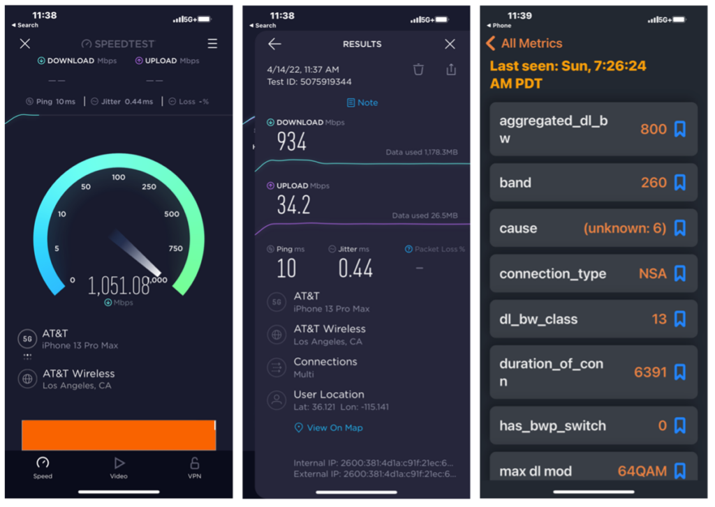
In the example shown below, conducted at John Wayne Airport in Orange County, California, the popular Speedtest by Ookla measured downloads of 1 Gbps and uploads of 34 Mbps. But how much of that throughput is attributable to mmWave? By consulting their 5G smartphone’s diagnostics, a tech-savvy user can discover the 5G NR band and use that to determine whether they’re enjoying the benefits of mmWave. Our example shows that the 5G NR band is 260, which equates to the 39 GHz mmWave band. This airport setting is not only indicative of the priority environments in the 5G mmWave rollout but that the impressive wireless gains are already available in real-world scenarios.

Why is mmWave the future of wireless?
As our anecdotal Speedtest results and the Super Bowl experience both demonstrate, this premium 5G service is valuable for many subscribers. In the airport, executives can take part in real-time video chats, download and upload large files or watch a movie while waiting for their flight. In the stadium, spectators can view replays in High Definition or share halftime videos. And they can do this while hundreds or even thousands of other users in their immediate proximity are doing the same. Without 5G and its additional spectrum for mitigating network congestion, subscribers in these same situations have found themselves effectively off-grid in the past.
Looking to the future, and as this use case illustrates, video and interactive video are driving innovation as well as consumer demand. Video already accounts for 70% of all mobile data traffic, and it’s projected to account for 80% by 2028. And even that remarkable projected growth might not fully account for emerging eXtended Reality (XR) video applications. For those unfamiliar with this term, XR involves enhancing or even replacing our view of the world through the overlay of text and/or graphics onto real-world scenes. The XR experience therefore spans augmented reality (AR), virtual reality (VR) and mixed reality (MR). This futuristic experience will rely heavily on network infrastructure and mass market devices that can support its incredible data requirements. However, when it comes to video applications in the sub-6 GHz bands, today’s 5G networks are more optimized for coverage than ultra-high-speed data.
We can already see tiny glimpses of the promise that XR holds. Just think of the current buzz around VR headsets or the utility of AR apps that can measure real-world spaces via your smartphone’s camera. The immersive experiences that evolve out of these early XR concepts are certain to transform the way we live and interact with each other around the world.
Unfortunately, at the moment these experiences are confined to controlled environments and small-scale applications. To realize their full potential, users will have to be fully untethered from cables and have ubiquitous access to XR. This presents a challenge that both network operators and device manufacturers will have to rise to meet. Creating a solid foundation for an XR-powered future will mean having to satisfy the growing needs of more and more subscribers for the low-latency, high-throughput connections that underpin ambitious XR technologies. This is the type of innovation that mmWave can enable.
5G smartphone architecture
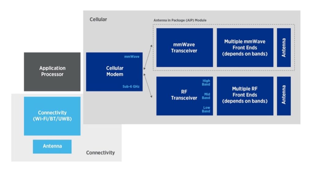
With that in mind, we now turn to the micro-level device architecture on which those massive technological shifts rest. The following block diagram offers a closer look at the mmWave wireless link within the 5G smartphone. Note the compartmentalization between connectivity and cellular paths. Also note the high-level similarities in the sub-6 GHz and mmWave paths, and how the antenna in package (AiP) module has the same general functionality as the more discrete sub-6 GHz path. The modem for both connectivity and cellular simplify to a digital core for modulation/demodulation functions. In addition, they are separated from the application processor that is at the core of every 5G smartphone. These, then, are the primary wireless building blocks that append to the application processor for wireless functionality — or, in other words, the untethered connectivity that will empower next-gen XR applications.

The following table outlines the fundamental antenna differences between the sub-6 GHz and mmWave paths to help explain why the mmWave frontend is more complex. This complexity stems from the phase array and beamforming functions.
| Sub-6GHz Antenna(s) | mmWave Antenna(s) |
| Multiple input multiple output (MIMO) is the key technology that overcomes bandwidth limitations by breaking a high-data-rate signal into multiple lower-rate streams. The antennas are not coupled. In fact, it is optimal to have the antennas separated from each other as much as possible. The fundamental control mechanism is limited to power adjustments only. | Phase arrays overcome low power or high losses by focusing the energy towards a desired direction. Beamforming is the key technology that enhances the link budget. In this approach, phase arrays have every single antenna element strongly coupled and transmitting the same signal. The fundamental control mechanisms are magnitude and phase that effectively steer the beam. |
The antenna in package (AiP) module
Any online teardown of a 5G smartphone reveals that the most innovative addition to the 5G architecture is the introduction of the separate mmWave chain to support those dedicated high-frequency bands. In this new mmWave link, the architecture isn’t all that dissimilar to the sub-6 GHz linkages. Here, too, there are transmit and receive paths. The mmWave link differs in that the AiP module converts to an intermediate frequency (IF) that the cellular modem can process more easily. This intermediate interface is given the designation 5G IF. In this way, the mmWave chain simplifies to a functional block that converts mmWave to 5G IF and therefore functionally acts similarly to the sub-6 GHz links.
Armed with this insight, we can see that the key differentiator between premium mmWave-enabled smartphones and economy RF-only variants is the presence of this mmWave functional block chain in the former. This highlights the modularity of 5G smartphone design, which in turn lends itself to the competitive mobile device market.
Closer inspection of the mmWave function block reveals the same prerequisite for antenna array (with beam-steering capabilities), transceiver, front-end and power management integrated circuit (PMIC) functions. Interestingly, at the mmWave frequencies, the geometrical dimensions prevent a single transceiver architecture from supporting both conventional sub-6 GHz bands and the 30+ GHz mmWave bands. Instead, these passive mmWave components, including antennae and antenna arrays, are comparable in size to radio-frequency integrated circuit (RFIC) packages or to the RFIC die itself. This small size allows for more advanced packaging possibilities with passive mmWave components bundled along with the active RFIC components. Furthermore, integrating the antennas along with the IC brings the added benefit of keeping transmission line losses to a minimum. This is necessary for increasing performance at mmWave frequencies.
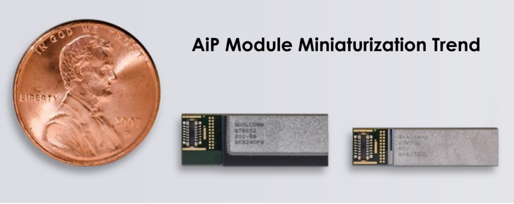
As the following promotional photo from Qualcomm shows, the antenna in package (AiP) module is undergoing miniaturization as it has become a strategic building block within the 5G smartphone. Careful placement of the AiP module around the perimeter of the 5G smartphone is necessary to minimize subscriber hand interference with the antenna elements. Worth noting is that the antenna array is integrated into the AiP module such that there are no mmWave conducted paths for test; only 5G IF is supported. Clearly, this AiP is an engineering marvel on many levels.

AiP module implications for test
Given the AiP module approach in the 5G smartphone architecture, we can formulate an overall test strategy framework based on insights from RF best practices. We offer six key takeaways regarding that test strategy:
- Minimizing cost of test (CoT) will require the fewest insertions for the mmWave AiP module.
- With each of these insertions, site density will proportionally affect economics. Higher site density equals lower CoT.
- The reliance on chiplets to satisfy miniaturization and packaging prerequisites impose a known-good-die (KGD) insertion on the transceiver IC during wafer test (see below). Put another way, this insertion needs to be more than just an electrical DC test. This poses a challenge to automated test equipment (ATE) given that mmWave instrument cost is much greater than traditional RF.
- Pogo pins are commonly used as an electrical connector mechanism during electronics testing. However, during wafer test, using these conventional spring-loaded pins is not possible at mmWave frequencies. The reason is because the pins act like inductive elements and hide the true performance of the transceiver. Instead, probes are necessary, which represents another ATE challenge.
- The packaging integration of a transceiver chiplet with an antenna array for beamforming imposes an over-the-air (OTA) insertion on the overall AiP module. This represents yet another ATE challenge, because this test method is more unavoidable when dealing with mmWave components on account of the antenna array integration.
- Loopback and built-in self-test (BIST) are currently being explored as alternative test strategies. However, given their current state of development, they introduce a real risk of shipping defective units. These test strategies also rely on extensive characterization activities and strict quality control mechanisms that must be incorporated at other points in the manufacturing process. Their lower upfront cost is offset by expensive remedial actions if — or when — defects elude capture.
To better visualize the optimal test strategy framework, we depict it here in a standard workflow format.

Make sure to read Part 2 of this article to for a deep dive into three of these important insertions.

