Even though most consumers are largely unaware of the unique elements in the 5G technology stack, the antenna in package (AiP) module inside the 5G smartphone is a prime enabler of mmWave technology — and is likewise the small but mighty force behind the performance enhancements that they enjoy when watching or interacting with video. Part 1 of this article explored how to test your mmWave link and how 5G smartphone architecture and the AiP module impacts test strategies. Part 2 builds on that conversation by exploring KGD insertion, Antenna PCB insertion and OTA insertion.
1. KGD insertion
As the following X-ray photo from TechInsights shows, the additive manufacturing process will need KGD to populate the AiP module. The justification here is that the expense of defects or failures in the next stage of assembly is widely acknowledged to be 10x more expensive than when captured beforehand. For this reason, the AiP module workflow requires a KGD insertion to essentially verify mmWave parameters (e.g., beamforming) at wafer test to separate good from bad transceivers.

2. Antenna PCB insertion
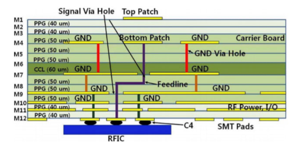
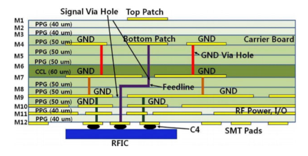
Similar to the KGD insertion, the printed circuit board (PCB) is a critical building block that contains the signal distribution, antenna elements, thermal relief, and stack interconnects. One AiP module design example is shown in Figure 6. Careful design and manufacture of the PCB is necessary to ensure overall performance of the AiP module. Yet this poses an ATE challenge because many of the emerging defect mechanisms are nearly imperceptible unless testing at actual mmWave frequencies. A typical stack-up is shown in the following figure to illustrate the complexity in the AiP PCB design,5 including the prerequisite for dielectric material (e.g., FR4). This complexity will likely impose the requirement for an OTA insertion to have adequate test coverage for possible defects in this PCB.

3. OTA insertion
The fully assembled AiP module will benefit from an OTA insertion to capture integration defects. The main prerequisite for OTA is an anechoic chamber, ideally with site density that satisfies CoT objectives using a standard handler. This OTA insertion will verify in-band performance, which spans both transmit and receive functions, and conduct error vector magnitude (EVM) measurements to reveal possible outliers in the manufacturing process. Furthermore, this vital insertion will satisfy out-of-band test criteria to ensure compliance with adjacent channel licensing terms.
Conclusion
On the network side, further mmWave deployments will be necessary to complete the mmWave wireless link. At the moment, this network infrastructure is concentrated in dense urban environments, and it will likely remain so until broader mmWave rollouts follow a similar trajectory to historical RF deployments and become more commonplace. While this mmWave infrastructure is being built out, emerging XR applications that leverage video content in novel ways will be at the forefront of the premium user scenarios that will drive future wireless standards, such as 6G and 7G.
Hardware manufacturers can make use of this time to develop and implement an mmWave test strategy that’s optimized for 5G and beyond. To be sure, mmWave testing is presently much more expensive and complex than sub-6GHz components. Test strategies are nevertheless evolving with a view to mitigating the defect mechanisms in the mmWave ecosystem, which in turn will accelerate the adoption of this innovative new technology and enable providers to offer exciting new premium services.

